The push for smaller, more sensitive, and more integrated sensors and biosensors necessitates advanced fabrication techniques, and at the heart of these lies lithography. These techniques, particularly photo-lithography and electron beam lithography (EBL), are fundamental to defining the very structure of sensor substrates, enabling the creation of devices with tailored functionalities and performance characteristics.
Lithography allows researchers to precisely pattern materials onto a substrate – silicon, glass, polymers, or flexible materials – creating the intricate features that define the sensor's active area, electrodes, micro-channels, and insulating layers.
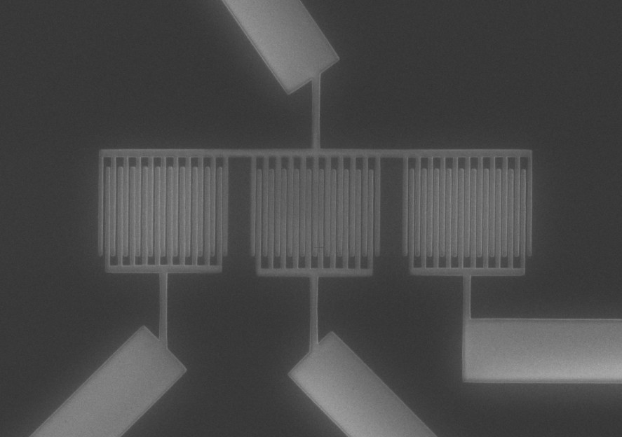
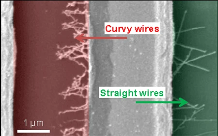
While photo-lithography is cost-effective and high-throughput, it's limited by the diffraction limit of light, restricting the minimum feature size. This is where EBL comes into play. EBL uses a focused electron beam to directly write patterns onto a resist, achieving resolutions down to a few nanometers. This is crucial for research pushing the boundaries of sensor miniaturization, creating nanoscale electrodes for single-molecule detection, or fabricating complex 3D structures for enhanced sensitivity.
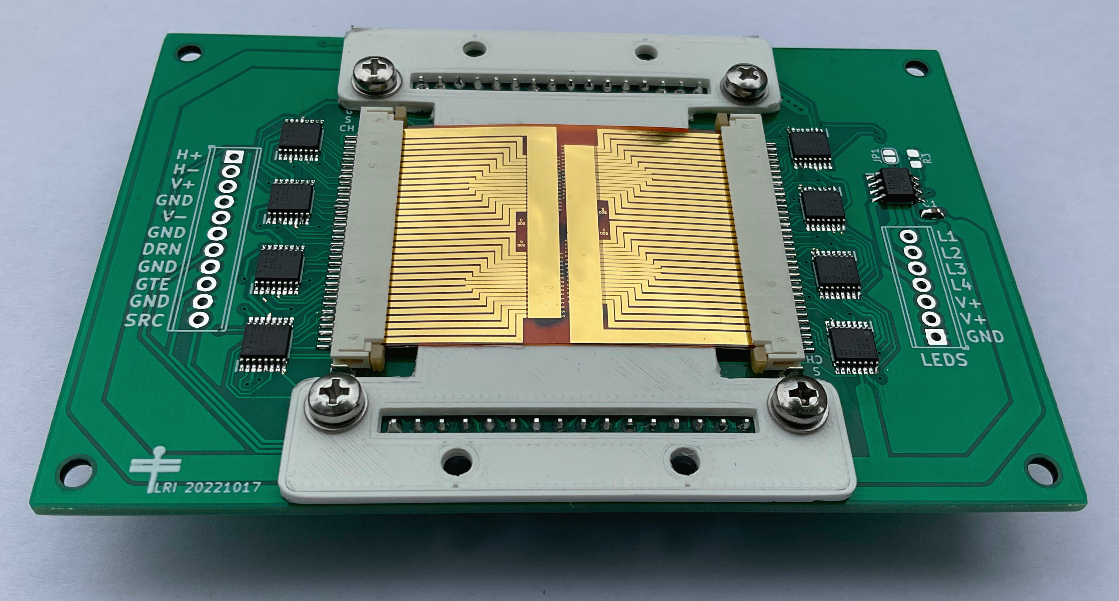
Fabricating the sensor is only half the battle. The signals generated by these microscopic sensors are typically weak and noisy. This is where electronics engineering becomes absolutely critical. The raw signal needs to be conditioned, amplified, filtered, and digitized before it can be meaningfully interpreted.
The advancement of sensor and biosensor technology is inextricably linked to the progress in both lithographic techniques for precise fabrication and electronics engineering for robust signal processing. These two disciplines work in synergy, enabling the creation of sophisticated and powerful sensing devices that are revolutionizing fields like healthcare, environmental monitoring, and industrial automation.
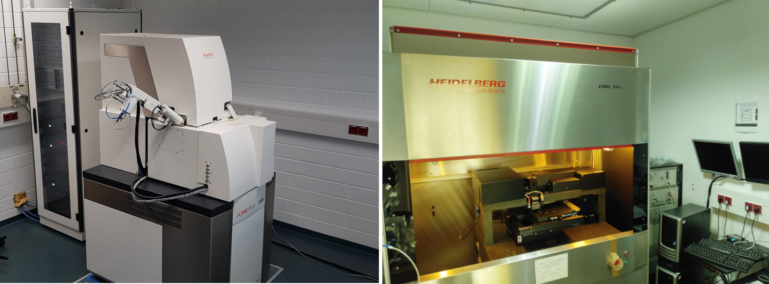
At the Chair of Material Science and Nanotechnology we have have state of the art photo lithography and electron-beam lithography equipment as well as well equipped electronics lab for the fabrication of advanced sensor technologies.


The push for smaller, more sensitive, and more integrated sensors and biosensors necessitates advanced fabrication techniques, and at the heart of these lies lithography. These techniques, particularly photo-lithography and electron beam lithography (EBL), are fundamental to defining the very structure of sensor substrates, enabling the creation of devices with tailored functionalities and performance characteristics.
Lithography allows researchers to precisely pattern materials onto a substrate – silicon, glass, polymers, or flexible materials – creating the intricate features that define the sensor's active area, electrodes, micro-channels, and insulating layers.
While photo-lithography is cost-effective and high-throughput, it's limited by the diffraction limit of light, restricting the minimum feature size. This is where EBL comes into play. EBL uses a focused electron beam to directly write patterns onto a resist, achieving resolutions down to a few nanometers. This is crucial for research pushing the boundaries of sensor miniaturization, creating nanoscale electrodes for single-molecule detection, or fabricating complex 3D structures for enhanced sensitivity.
Fabricating the sensor is only half the battle. The signals generated by these microscopic sensors are typically weak and noisy. This is where electronics engineering becomes absolutely critical. The raw signal needs to be conditioned, amplified, filtered, and digitized before it can be meaningfully interpreted.
The advancement of sensor and biosensor technology is inextricably linked to the progress in both lithographic techniques for precise fabrication and electronics engineering for robust signal processing. These two disciplines work in synergy, enabling the creation of sophisticated and powerful sensing devices that are revolutionizing fields like healthcare, environmental monitoring, and industrial automation.
At the Chair of Material Science and Nanotechnology we have have state of the art photo lithography and electron-beam lithography equipment as well as well equipped electronics lab for the fabrication of advanced sensor technologies.