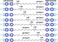
Understanding the charge transport mechanisms in nanoscale structures is essential for the development of molecular electronic devices. Charge transport through one-dimensional (1D) molecular systems connected between two contacts is influenced by several parameters, such as the electronic structure of the molecule and the presence of disorder and defects. In this work, we have modeled 1D molecular wires connected between electrodes and systematically investigated the influence of both soliton formation and the presence of defects on properties such as conductance and the density of states. Our numerical calculations have shown that the transport properties are highly sensitive to the positions of both the solitons and the defects. Interestingly, the introduction of a single defect in the molecular wire that divides it into two fragments, both consisting of an odd number of sites, creates a new conduction channel at the center of the band gap, resulting in higher zero-bias conductance than for defect-free systems. This phenomenon suggests alternative routes for the engineering of molecular wires with enhanced conductance.

Understanding the charge transport mechanisms in nanoscale structures is essential for the development of molecular electronic devices. Charge transport through one-dimensional (1D) molecular systems connected between two contacts is influenced by several parameters, such as the electronic structure of the molecule and the presence of disorder and defects. In this work, we have modeled 1D molecular wires connected between electrodes and systematically investigated the influence of both soliton formation and the presence of defects on properties such as conductance and the density of states. Our numerical calculations have shown that the transport properties are highly sensitive to the positions of both the solitons and the defects. Interestingly, the introduction of a single defect in the molecular wire that divides it into two fragments, both consisting of an odd number of sites, creates a new conduction channel at the center of the band gap, resulting in higher zero-bias conductance than for defect-free systems. This phenomenon suggests alternative routes for the engineering of molecular wires with enhanced conductance.
