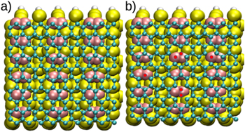
In this work, we show the doping of graphene most likely from heteroatoms induced by the substrate using Raman spectra, x-ray photoelectron spectroscopy, energy dispersive x-ray spectroscopy and ab initio molecular dynamics (MD) simulations. The doping of graphene on a highly boron-doped silicon substrate was achieved by an annealing at 400 K for about 3 h in an oven with air flow. With the same annealing, only the Raman features similar to that from the pristine graphene were observed in the freestanding graphene and the graphene on a typical Si/SiO2 wafer. Ab initio MD simulations were performed for defected graphene on boron-doped silicon substrate at several temperatures. All vacancy sites in the graphene are occupied either with B atoms or Si atoms resulting in the mixed boron-silicon doping of the graphene. The MD simulations validated the experimetal finding of graphene doped behavior observed by Raman spectrum. The electronic structure analysis indicated the p-type nature of doped graphene. The observed doping by the possible incorporation of heteroatoms into the graphene, simply only using 400 K annealing the boron-doped Si substrate, could provide a new approach to synthesize doped graphene in a more economic way.

In this work, we show the doping of graphene most likely from heteroatoms induced by the substrate using Raman spectra, x-ray photoelectron spectroscopy, energy dispersive x-ray spectroscopy and ab initio molecular dynamics (MD) simulations. The doping of graphene on a highly boron-doped silicon substrate was achieved by an annealing at 400 K for about 3 h in an oven with air flow. With the same annealing, only the Raman features similar to that from the pristine graphene were observed in the freestanding graphene and the graphene on a typical Si/SiO2 wafer. Ab initio MD simulations were performed for defected graphene on boron-doped silicon substrate at several temperatures. All vacancy sites in the graphene are occupied either with B atoms or Si atoms resulting in the mixed boron-silicon doping of the graphene. The MD simulations validated the experimetal finding of graphene doped behavior observed by Raman spectrum. The electronic structure analysis indicated the p-type nature of doped graphene. The observed doping by the possible incorporation of heteroatoms into the graphene, simply only using 400 K annealing the boron-doped Si substrate, could provide a new approach to synthesize doped graphene in a more economic way.
