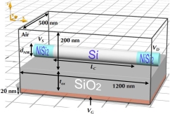
We present a theoretical framework for the calculation of charge transport through nanowire-based Schottky-barrier field-effect transistors that is conceptually simple but still captures the relevant physical mechanisms of the transport process. Our approach combines two approaches on different length scales: (1) the finite elements method is used to model realistic device geometries and to calculate the electrostatic potential across the Schottky-barrier by solving the Poisson equation, and (2) the Landauer approach combined with the method of non-equilibrium Green functions is employed to calculate the charge transport through the device. Our model correctly reproduces typical I-V characteristics of field-effect transistors and the dependence of the saturated drain current on the gate field and the device geometry are in good agreement with experiments. Our approach is suitable for one-dimensional Schottky-barrier field-effect transistors of arbitrary device geometry and it is intended to be a simulation platform for the development of nanowire-based sensors.

We present a theoretical framework for the calculation of charge transport through nanowire-based Schottky-barrier field-effect transistors that is conceptually simple but still captures the relevant physical mechanisms of the transport process. Our approach combines two approaches on different length scales: (1) the finite elements method is used to model realistic device geometries and to calculate the electrostatic potential across the Schottky-barrier by solving the Poisson equation, and (2) the Landauer approach combined with the method of non-equilibrium Green functions is employed to calculate the charge transport through the device. Our model correctly reproduces typical I-V characteristics of field-effect transistors and the dependence of the saturated drain current on the gate field and the device geometry are in good agreement with experiments. Our approach is suitable for one-dimensional Schottky-barrier field-effect transistors of arbitrary device geometry and it is intended to be a simulation platform for the development of nanowire-based sensors.
