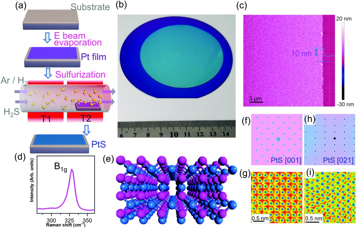
2D nonlayered materials have attracted enormous research interests due to their novel physical and chemical properties with confined dimensions. Platinum monosulfide as one of the most common platinum-group minerals has been less studied due to either the low purity in the natural product or the extremely high-pressure conditions for synthesis. Recently, platinum monosulfide (PtS) 2D membranes have emerged as rising-star materials for fundamental Raman and X-ray photoelectron spectral analysis as well as device exploration. However, a large-area homogeneous synthesis route has not yet been proposed and released. In this communication, we report a facile metal sulfurization strategy for the synthesis of a 4-inch wafer-scale PtS film. Enhanced characterization tools have been employed for thorough analysis of the crystal structure, chemical environment, vibrational modes, and atomic configuration. Furthermore, through theoretical calculations the phase diagram of the Pt–S compound has been plotted for showing the successful formation of PtS in our synthesis conditions. Eventually, a high-quality PtS film has been reflected in device demonstration by a photodetector. Our approach may shed light on the mass production of PtS films with precise control of their thickness and homogeneity as well as van der Waals heterostructures and related electronic devices.

2D nonlayered materials have attracted enormous research interests due to their novel physical and chemical properties with confined dimensions. Platinum monosulfide as one of the most common platinum-group minerals has been less studied due to either the low purity in the natural product or the extremely high-pressure conditions for synthesis. Recently, platinum monosulfide (PtS) 2D membranes have emerged as rising-star materials for fundamental Raman and X-ray photoelectron spectral analysis as well as device exploration. However, a large-area homogeneous synthesis route has not yet been proposed and released. In this communication, we report a facile metal sulfurization strategy for the synthesis of a 4-inch wafer-scale PtS film. Enhanced characterization tools have been employed for thorough analysis of the crystal structure, chemical environment, vibrational modes, and atomic configuration. Furthermore, through theoretical calculations the phase diagram of the Pt–S compound has been plotted for showing the successful formation of PtS in our synthesis conditions. Eventually, a high-quality PtS film has been reflected in device demonstration by a photodetector. Our approach may shed light on the mass production of PtS films with precise control of their thickness and homogeneity as well as van der Waals heterostructures and related electronic devices.
