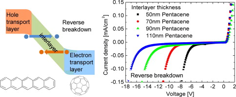
Charge carrier transport under reverse voltage conditions is of major relevance in devices like organic photo-detectors, organic solar cells (tandem cells), organic light emitting diodes (generation contacts), and organic Zener diodes. We present organic pin-diodes comprising molecular doped layers of pentacene and C60 with an adjustable and reversible reverse breakdown behavior. We discuss the electric field and temperature dependence of the breakdown mechanism and propose a coherent charge transport scenario to describe the experimental findings. Within this model a field assisted tunneling of charge carriers over a rather large distance from valence to conductance states (and vice versa) governs the breakdown behavior. This is in accordance to experimental observations where charge carriers can overcome a layer thickness of 110 nm in the breakdown regime.

Charge carrier transport under reverse voltage conditions is of major relevance in devices like organic photo-detectors, organic solar cells (tandem cells), organic light emitting diodes (generation contacts), and organic Zener diodes. We present organic pin-diodes comprising molecular doped layers of pentacene and C60 with an adjustable and reversible reverse breakdown behavior. We discuss the electric field and temperature dependence of the breakdown mechanism and propose a coherent charge transport scenario to describe the experimental findings. Within this model a field assisted tunneling of charge carriers over a rather large distance from valence to conductance states (and vice versa) governs the breakdown behavior. This is in accordance to experimental observations where charge carriers can overcome a layer thickness of 110 nm in the breakdown regime.
