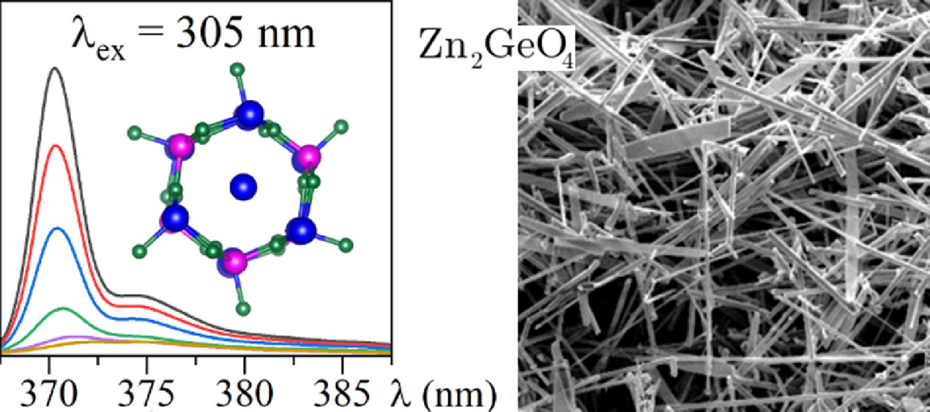
Achieving efficient and stable ultraviolet emission is a challenging goal in optoelectronic devices. Herein, we investigate the UV luminescence of zinc germanate Zn2GeO4 microwires by means of photoluminescence measurements as a function of temperature and excitation conditions. The emitted UV light is composed of two bands (a broad one and a narrow one) associated with the native defects structure. In addition, with the aid of density functional theory (DFT) calculations, the energy positions of the electronic levels related to native defects in Zn2GeO4 have been calculated. In particular, our results support that zinc interstitials are the responsible for the narrow UV band, which is, in turn, split into two components with different temperature dependence behaviour. The origin of the two components is explained on the basis of the particular location of Zni in the lattice and agrees with DFT calculations. Furthermore, a kinetic luminescence model is proposed to ascertain the temperature evolution of this UV emission. These results pave the way to exploit defect engineering in achieving functional optoelectronic devices to operate in the UV region.

Achieving efficient and stable ultraviolet emission is a challenging goal in optoelectronic devices. Herein, we investigate the UV luminescence of zinc germanate Zn2GeO4 microwires by means of photoluminescence measurements as a function of temperature and excitation conditions. The emitted UV light is composed of two bands (a broad one and a narrow one) associated with the native defects structure. In addition, with the aid of density functional theory (DFT) calculations, the energy positions of the electronic levels related to native defects in Zn2GeO4 have been calculated. In particular, our results support that zinc interstitials are the responsible for the narrow UV band, which is, in turn, split into two components with different temperature dependence behaviour. The origin of the two components is explained on the basis of the particular location of Zni in the lattice and agrees with DFT calculations. Furthermore, a kinetic luminescence model is proposed to ascertain the temperature evolution of this UV emission. These results pave the way to exploit defect engineering in achieving functional optoelectronic devices to operate in the UV region.
