Nanocrystals (NCs) are excellent candidates to be used as fluorophores in biosensing applications due to their high thermal and photochemical stability, as well as the extraordinary optical properties. The role and functionality of NCs in biosensing systems can range from simple fluorescent tags to intrinsic sensors that utilize the photophysical response of NCs to the external stimuli. Due to their high color purity and exceptional emitting properties, they can act as donors, acceptors, or both in energy transfer-based biosensing systems, e.g., förster resonance energy transfer (FRET). They also provide great versatility for the design and fabrication of novel sensing platforms. To make use of colloidal NCs in practical sensing devices, the preparation of micro-/nanoarrays of NCs with device suitable thickness is necessary. Such structures with multiplexed functionalities are of a broad interest in the field of nanophotonics and cellular dynamics.
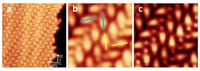
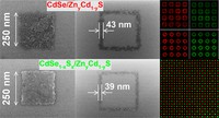
They can provide innovative experimental platforms to investigate biological interactions as well as FRET-based studies. Several strategies, including microdroplet inject-printing, microcontact printing, electro-hydrodynamic printing, and bubble printing, have been developed and reported to fabricate micro-/nanopatterned structures of NCs during the past decade. Among the various reported microfabrication approaches, direct patterning of NCs using electron beam lithography (EBL) has demonstrated itself as an attractive, highly accurate technique to produce geometrically defined multilayer features with high resolution and fidelity. Here in the "Nanomaterials for Sensor Technologies" research-line, we have focused on direct EBL of colloidal semiconductor NCs. These nano-patterned structures can be utilized as innovative experimental platforms to investigate biological interactions and biomolecular studies or be adopted in multiplex FRET-based biosensing applications.
Nanopatterning
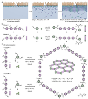
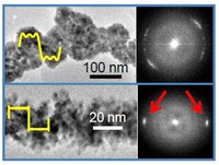
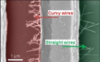
Due to ease of fabrication of arbitrary structures with high specificity as well as the “direct” writing of the desired pattern on the substrate, electron-beam lithography (EBL) has attracted significant attention and the micro-/nanopatterned surfaces generated by this technique are excellent candidates to be integrated into solid-state devices such as biosensors. Compared to traditional photolithography, EBL does not suffer from the drawbacks of conventional methods such as roughness generation during the etching step, long processing times, or resist/film adhesion and can achieve much better resolutions due to an extremely short wavelength of the electron beam (0.2-0.5 Å). This method is a versatile and straightforward tool to fabricate nanoscale features that meet the requirements of nanophotonic studies.

Biosensing
The energy transfer mechanism is one of the most common sensing mechanisms that can be categorized into two main classes: resonance energy transfer (RET) or electron transfer (eT). The Förster resonance energy transfer (FRET) is the most investigated and well-known mechanism in biosensing and includes a distance-dependent non-radiative energy transfer from an excited donor to an acceptor through dipole-dipole resonance. Depend on the origin of excitation; RET mechanism can be classified into fluorescence/luminescence RET (FRET/LRET), where the donor excited-state is generated through optical excitation, chemiluminescence RET (CRET), where the excited state donor is created through a chemical reaction, and bioluminescent RET (BRET), where the excited state donor is created through a biochemical reaction.
Nanocrystals (NCs) are excellent candidates to be used as fluorophores in biosensing applications due to their high thermal and photochemical stability, as well as the extraordinary optical properties. The role and functionality of NCs in biosensing systems can range from simple fluorescent tags to intrinsic sensors that utilize the photophysical response of NCs to the external stimuli. Due to their high color purity and exceptional emitting properties, they can act as donors, acceptors, or both in energy transfer-based biosensing systems, e.g., förster resonance energy transfer (FRET). They also provide great versatility for the design and fabrication of novel sensing platforms. To make use of colloidal NCs in practical sensing devices, the preparation of micro-/nanoarrays of NCs with device suitable thickness is necessary. Such structures with multiplexed functionalities are of a broad interest in the field of nanophotonics and cellular dynamics.
They can provide innovative experimental platforms to investigate biological interactions as well as FRET-based studies. Several strategies, including microdroplet inject-printing, microcontact printing, electro-hydrodynamic printing, and bubble printing, have been developed and reported to fabricate micro-/nanopatterned structures of NCs during the past decade. Among the various reported microfabrication approaches, direct patterning of NCs using electron beam lithography (EBL) has demonstrated itself as an attractive, highly accurate technique to produce geometrically defined multilayer features with high resolution and fidelity. Here in the "Nanomaterials for Sensor Technologies" research-line, we have focused on direct EBL of colloidal semiconductor NCs. These nano-patterned structures can be utilized as innovative experimental platforms to investigate biological interactions and biomolecular studies or be adopted in multiplex FRET-based biosensing applications.
Nanopatterning
Due to ease of fabrication of arbitrary structures with high specificity as well as the “direct” writing of the desired pattern on the substrate, electron-beam lithography (EBL) has attracted significant attention and the micro-/nanopatterned surfaces generated by this technique are excellent candidates to be integrated into solid-state devices such as biosensors. Compared to traditional photolithography, EBL does not suffer from the drawbacks of conventional methods such as roughness generation during the etching step, long processing times, or resist/film adhesion and can achieve much better resolutions due to an extremely short wavelength of the electron beam (0.2-0.5 Å). This method is a versatile and straightforward tool to fabricate nanoscale features that meet the requirements of nanophotonic studies.
Biosensing
The energy transfer mechanism is one of the most common sensing mechanisms that can be categorized into two main classes: resonance energy transfer (RET) or electron transfer (eT). The Förster resonance energy transfer (FRET) is the most investigated and well-known mechanism in biosensing and includes a distance-dependent non-radiative energy transfer from an excited donor to an acceptor through dipole-dipole resonance. Depend on the origin of excitation; RET mechanism can be classified into fluorescence/luminescence RET (FRET/LRET), where the donor excited-state is generated through optical excitation, chemiluminescence RET (CRET), where the excited state donor is created through a chemical reaction, and bioluminescent RET (BRET), where the excited state donor is created through a biochemical reaction.